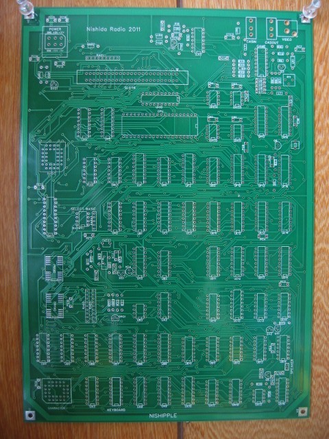
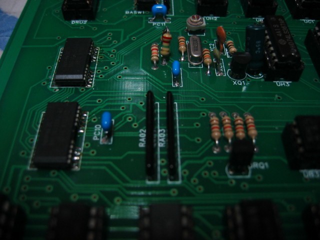
print circuit board♡
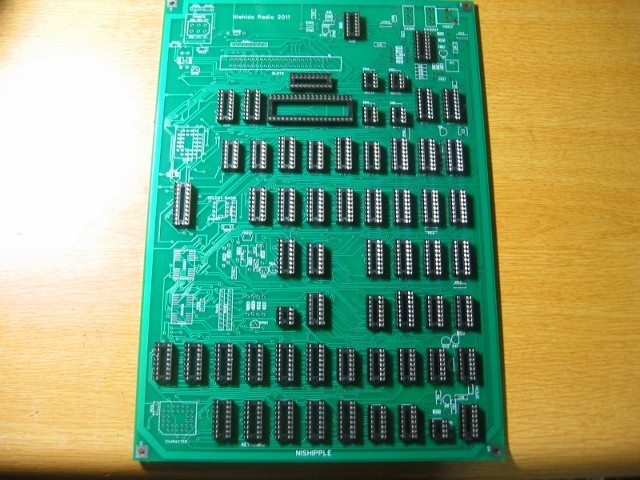
soldering♥
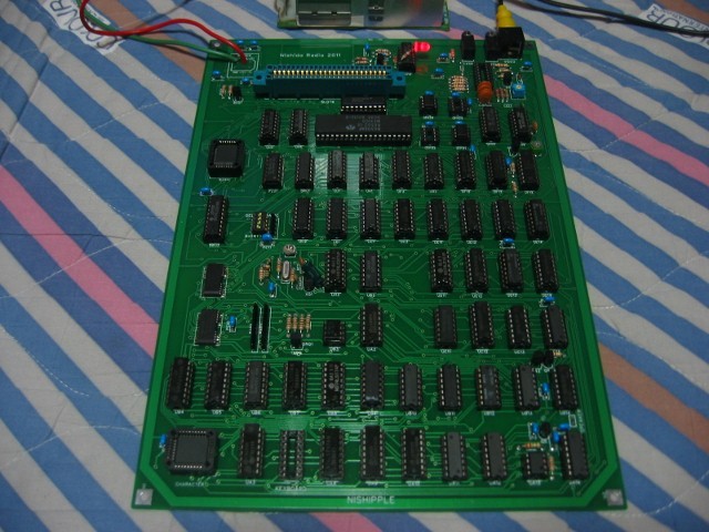
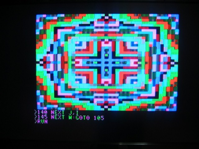
finished☆
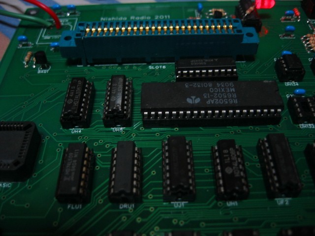
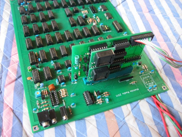
6502 micro processor! there is only one slot.
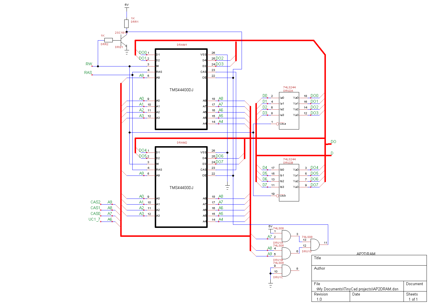
junk DRAM is reused.
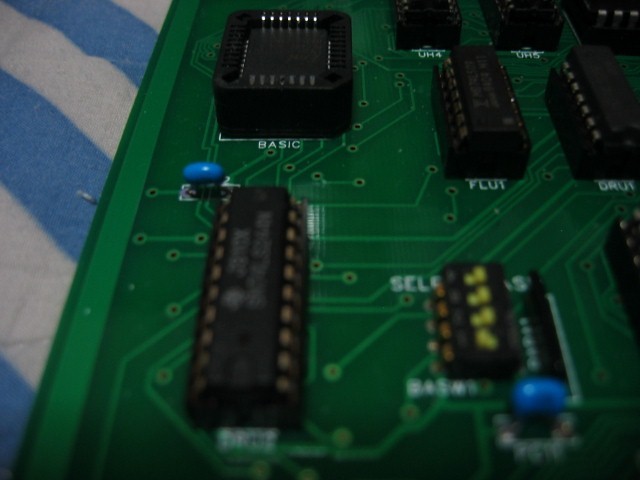
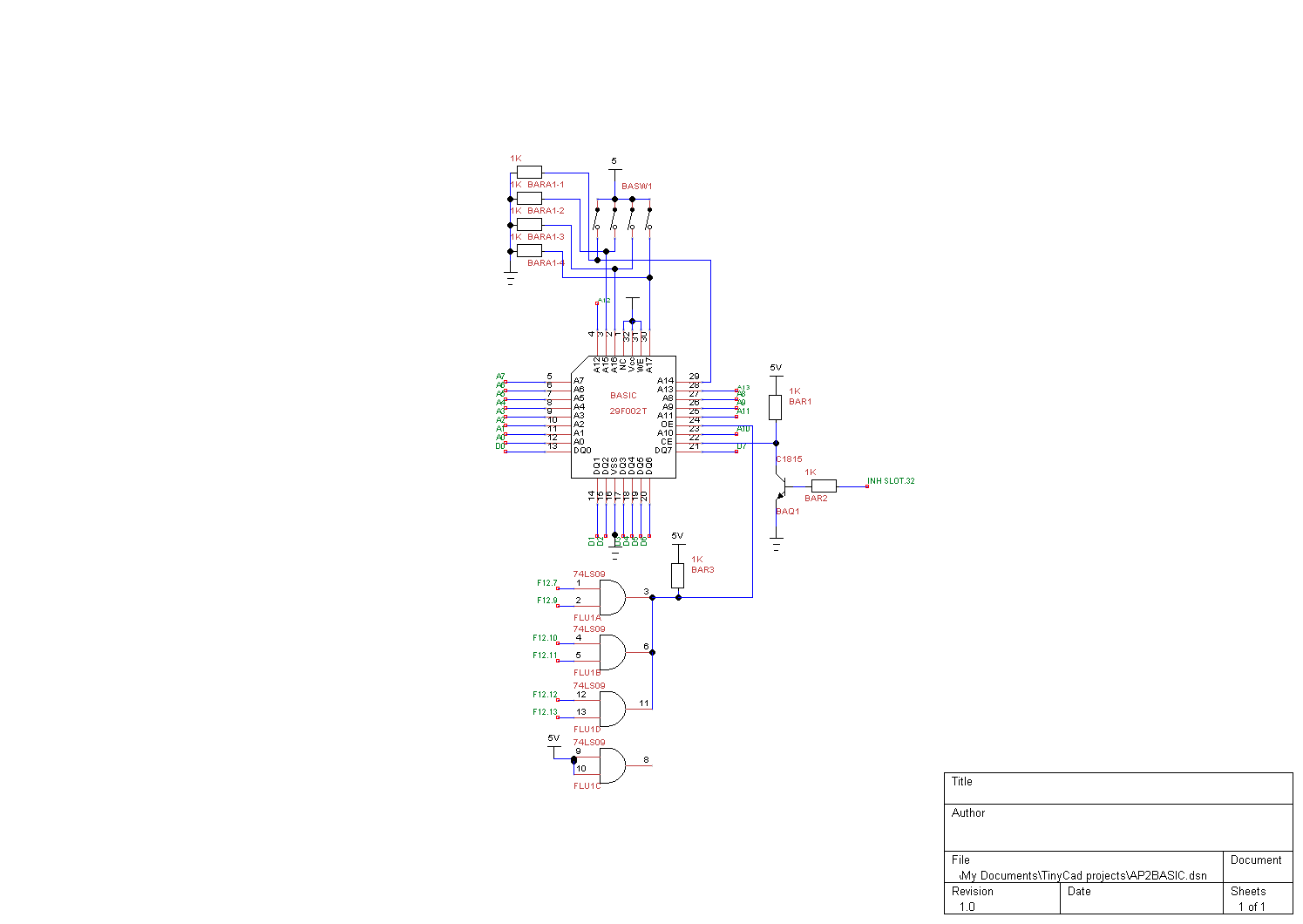
BASIC ROM written in a flash. You can select a ROM image from 16 images.
This is a construction kit of A*p*e II compatible logic board.
print circuit board♡ |
soldering♥ |
finished☆ |
6502 micro processor! there is only one slot. |
junk DRAM is reused. |
BASIC ROM written in a flash. You can select a ROM image from 16 images. |
Based on II Plus circuit except the followings.
BASIC ROM
DRAM
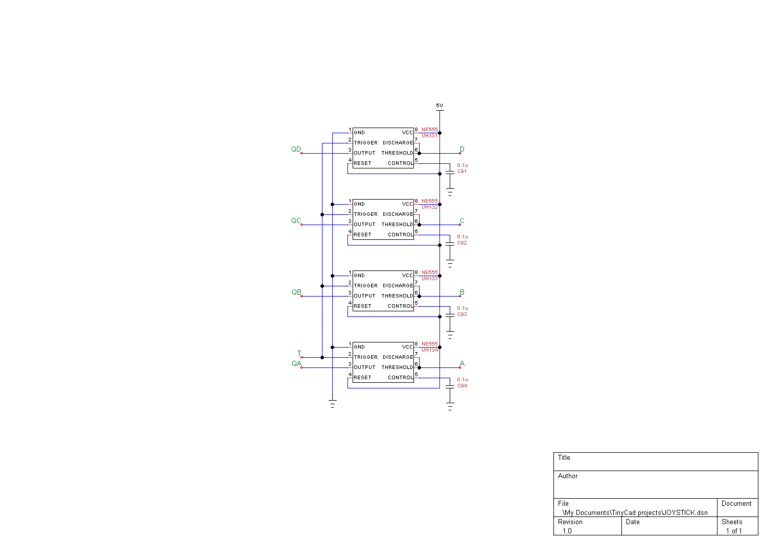
joystick
oscillator
cassette input
Place a ROM image on the address from 1000h to 3FFFh (12K bytes). Place dummy data from 0000h to 0FFFh.
If you want to use multiple ROM images, place data as the following.
DUMMY : 0000h - 0FFFh
ROM0 : 1000h - 3FFFh
DUMMY : 4000h - 4FFFh
ROM1 : 5000 - 7FFFh
DUMMY : 8000 - 8FFFh
ROM2 : 9000 - BFFFh
Write data from the beginning of EN29F002T.
When you write an image using a EN29F002T Flash Memory Writer, make the total length exactly 256K bytes by adding dummy data.
| CPU, flash ROM, DRAM | |
| CHARACTER | EN29F002T |
| BASIC | EN29F002T |
| DRAM1-2 | TMS44400DJ etc. |
| CPU | 6502 |
| transistors and diodes | |
| Q5 | 2SC1815 |
| Q42 | 2SC1815 |
| Q41 | 2SC1815 |
| DRQ1 | 2SC1815 |
| XQ1 | 2SC1815 |
| Q6 | 2SC1815 |
| BAQ1 | 2SC1815 |
| Q3 | 2SC1815 |
| CR1 | 1S2076 etc. |
| CTQ1 | 2SC1815 |
| generic ICs | |
| UA3 | 74LS166 |
| UA8 | 74LS257 |
| UA9 | 74LS151 |
| UA10 | 74LS194 |
| UA11 | 74LS74 |
| UA12 | 74LS02 |
| UA13 | NE555 |
| UA14 | 74LS02 |
| UB4 | 74LS194 |
| UB5 | 74LS174 |
| UB6 | 74LS257 |
| UB7 | 74LS257 |
| UB8 | 74LS174 |
| UB9 | 74LS194 |
| UB10 | 74LS74 |
| UB11 | 74LS08 |
| UB12 | 74LS11 |
| UB13 | 74LS02 |
| UB14 | 74LS02 |
| UB3 | NE555 |
| UA2 | 74LS00 |
| UC11 | 74LS04 |
| UC12 | 74LS257 |
| UC13 | 74LS51 |
| UC14 | 74LS32 |
| UH3 | 74LS367 |
| UB2 | 74F86 |
| UD11 | 74LS161 |
| UD12 | 74LS161 |
| UD13 | 74LS161 |
| UD14 | 74LS161 |
| DRU2 | 74LS244 |
| UH2 | 74LS138 |
| UB1 | 74LS175 |
| UC1 | 74LS153 |
| UC2 | 74LS195 |
| UE11 | 74LS153 |
| UE12 | 74LS153 |
| UE13 | 74LS153 |
| UE14 | 74LS283 |
| FLU1 | 74LS09 |
| DRU1 | 74LS08 |
| UJ1 | 74LS257 |
| UH1 | 74LS08 |
| UF2 | 74LS139 |
| UD2 | 74LS20 |
| UF12 | 74LS138 |
| UF13 | 74LS138 |
| UF14 | 74LS259 or 9334 |
| UH4 | 74LS367 |
| UH5 | 74LS367 |
| UH131-134 | NE555 |
| UH12 | 74LS138 |
| UH14 | 74LS251 |
| UH10 | 74LS245 |
| UJ13 | 74LS74 |
| LCRs | |
| PC9 | 0.1uF |
| R14 | 1KΩ |
| R26 | 2.2MΩ |
| PC1 | 0.1uF |
| C4 | 0.1uF |
| C12 | 0.1uF |
| PC2 | 0.1uF |
| R25 | 33Ω |
| PC10 | 0.1uF |
| RA02 | 1KΩ x 8 elements |
| RA03 | 1KΩ x 8 elements |
| DRR1 | 1KΩ |
| DRR2 | 1KΩ |
| R32 | 1KΩ |
| R31 | 1KΩ |
| PC3 | 0.1uF |
| R12 | 12KΩ |
| R13 | 3.3MΩ |
| C15 | 0.1uF |
| XR2 | 10KΩ |
| XR1 | 10KΩ |
| XC1 | 100PF |
| XC2 | 100PF |
| XR3 | 51Ω |
| XC4 | 10uF EC |
| XC3 | 30PF Trimmer (white) |
| PC11 | 0.1uF |
| PC4 | 0.1uF |
| BARA1 | 1KΩ x 4 elements |
| PC12 | 0.1uF |
| R5 | 1KΩ |
| PC5 | 0.1uF |
| R27 | 4.7KΩ |
| PC6 | 0.1uF |
| C3 | 50PF Trimmer (green) |
| C92 | 0.1uF |
| C91 | 0.1uF |
| C38 | 0.01uF |
| C2 | 47PF |
| L1 | 27uH |
| PC8 | 0.1uF |
| C94 | 0.1uF |
| C93 | 0.1uF |
| C7 | 0.022uF |
| C8 | 0.022uF |
| C5 | 0.022uF |
| C6 | 0.022uF |
| R6 | 2.7KΩ |
| R8 | 2KΩ |
| R7 | 1.5KΩ |
| R11 | 200Ω VR |
| R23 | 100Ω |
| R20 | 100Ω |
| R21 | 100Ω |
| R22 | 100Ω |
| R33 | 1KΩ |
| C11 | 0.1uF |
| R9 | 10Ω |
| R24 | 47KΩ |
| R10 | 33Ω |
| PC7 | 0.1uF |
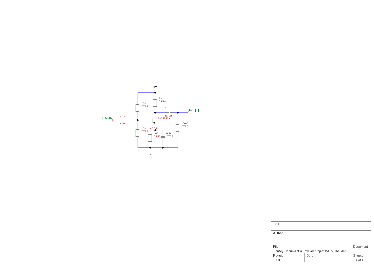
| CTC3 | 0.1uF |
| CTR5 | 100KΩ |
| L7 | short |
| BAR3 | 1KΩ |
| BAR1 | 1KΩ |
| PC14 | 0.1uF |
| PC13 | 0.1uF |
| BAR2 | 1KΩ |
| RA01 | 1KΩ x 8 elements |
| PC15 | 0.1uF |
| PC16 | 0.1uF |
| CTR1 | 10KΩ |
| CTR4 | 2KΩ |
| C10 | 0.1uF |
| CTR2 | 10KΩ |
| CTC2 | 0.1uF |
| CTR3 | 100Ω |
| R18 | 100Ω |
| R19 | 12KΩ |
| other | |
| XTAL | 14.318 MHz |
| BASW1 | 4 elements DIP switch |
| VIDEO | RCA Jack |
| CASIN | 3.5 mm mono jack |
| CASOUT | 3.5 mm mono jack |
| SLOT6 | 50 pin edge connector socket |
Other parts : 1 40pin DIP socket, 2 20pin sockets, 35 16pin DIP sockets, 18 14pin DIP sockets, 6 8pin DIP sockets
Working✿
Prepare a power supply more than 5V 2A. You only need 5V when you use the board with SDISK II and Apple II Plus keyboard adapter.
About the slot, Pin 1 is back right.
When you use an auto start ROM image, it doesn't work if you turn on the power immediately after turning off the power. It is because DRAM capaciter discharge is slower. Wait for a while and turn on the power again.